Glade Reference
The Schematic Editor is activated when a cellView with viewType 'schematic' is opened. The viewType is set when the cellView is created, for example using the File->New Cell command. The Schematic Editor is used to create and edit schematics. These can be netlisted for use in a simulator such as Spice, or to create layout in Glade. The formatting of the netlist is controlled by properties on the schematic symbol masters, using values from properties on the symbol instances.
A library of symbols must exist in order to place and wire devices in the schematic. A library of simple pins and power/ground symbols is provided in the 'basic' library. This is automatically loaded when Glade starts. The 'basic' library is required by the Create Pin command in schematics.
Schematic entry and editing does not require any specific technology file information - schematics use predefined system layers. For portability, it is recommended that the user does not use non-system layers in schematics or symbols.
The typical steps involved in creating a schematic are as follows:
Schematic editing shares many common menu entries with layout and symbol editing. Those specific to schematic are listed below.
Toggles the ignoring of selected schematic instances. The nlAction property is created and set to 'ignore' if the property does not exist. If it does exist, the property is deleted. Instances with the nlAction property set are shown in the schematic editor with a red cross.
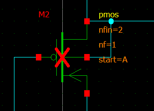
The netlisters will ignore any instances with this property set, so you can have e.g. dummy devices in the schematic that are not netlisted.
Displays the Create Instance dialog, which can be shown or hidden by the F3 key. An outline of the device instance is shown as the cursor is moved.
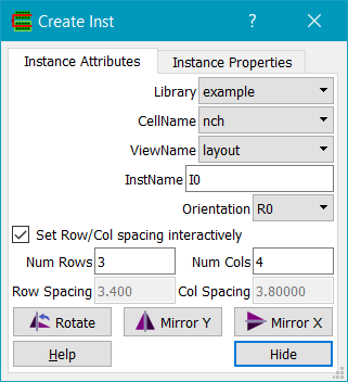
The instance name (InstName) is auto generated. If the Display Options 'Force Spice Compatible' radio button is checked, instance names are created using prefix characters suitable for Spice (M for mosfets, Q for bipolar devices, R for resistors etc). Otherwise instance name prefix is I followed by a number, or you can enter a more meaningful name. If you want to create an arrayed (bus) instance, use a suffix of <start_bit:stop_bit> where start_bit is the starting bit number and stop_bit is the stopping bit number, for example reg_array<7:0>
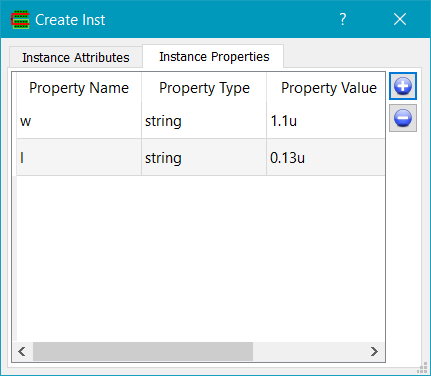
When an instance e.g. of an nmos device is entered, its properties such as W, L can be set using the Instance Properties tab on the dialog.
Creates a wire, starting at the initial point (either the current cursor position, if infix mode is on) or by a first point entered by a left mouse click. Subsequent left mouse clicks add wire end points; use the backspace key to back up an entered point, and use the return key or double click to end a wire. If the wire starts or ends on another wire midpoint, a solder dot is automatically entered at the junction of the two wires. If the wire starts or ends on the endpoint of an existin wire, the two wires will be merged into a single continuous wire. If you click on a pin (either an IO pin or a device pin) or click on a wire, the wire entry is ended. The snap direction can be set in the Create Wire dialog.
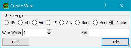
Snap Angle sets the snap direction when entering a wire.
Wire Width sets the display width of the wire. A value of 0 or 1 means 1 pixel wide. Net can be used to preset the net name for the wire; it is not necessary in most cases as subsequent Check CellView command will extract connectivity.
Creates a solder dot at the point entered by the cursor. If you want to connect two crossing wires, use a solder dot, else they are assumed to be bridging and not connected. The size of the dot can be set from the Display Options dialog.
Creates a label for the wire. The Create Label dialog will be displayed.
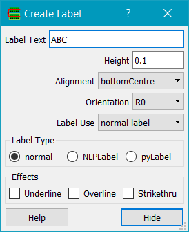
The Create Label dialog allows the name of the Label Text (i.e. net name) for the wire to be entered, along with Height, Orientation, Presentation. Label Use sets the use of the label; for layout and schematic views this should be 'normal label'. For symbols, choosing a different use sets the layer the label is created on. Label Type sets the label type. A normal type label displays its label text as is. A NLPLabel label has the label text evaluated as an NLP expression. A pyLabel has its text evaluated as a Python expression. Effects sets label effects such as Underline, Overline and Strikethru. Note that label effects, although displayed visually, cannot be represented in many external formats.They are mainly useful for schematics/symbols.
For bus wires, names are of the format name<start_bit:stop_bit>, where start_bit is the stating bit number and stop_bit is the stopping bit number, for example address<15:0>
Displays the Create Schematic Pin dialog.
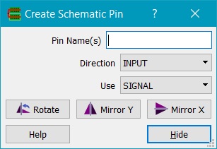
A list of Pin Name(s) can be entered, separated by spaces. As each pin is positioned by left clicking, a pin of the first name in the pin name list is created, and that name is removed from the list of pin names. The pin Direction and pin Use can also be specified. Pins can be mirrored or rotated during entry. A pin is actually an instance of a pin from the 'basic' library; if this library cannot be opened when Glade starts an error will be reported and Create Pin will fail.
For bus pins, names are of the format name<start_bit:stop_bit>, where start_bit is the stating bit number and stop_bit is the stopping bit number, for example data<0:7>
Create->Create CellView from CellView
Displays the Create CellView dialog.
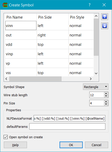
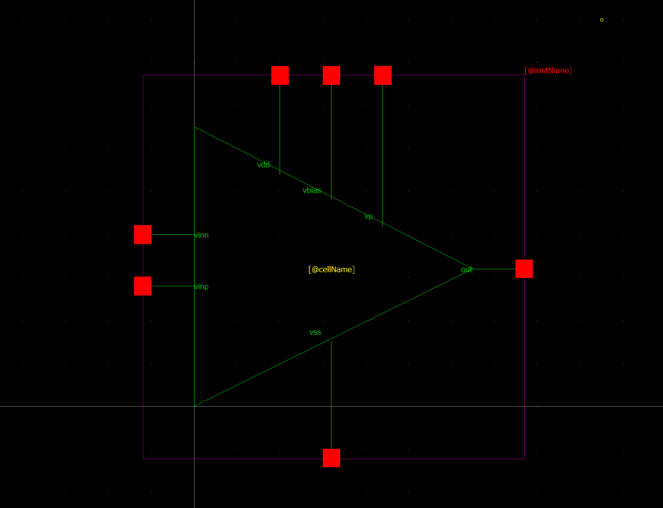
The Create Cellview from Cellview command creates a symbol view from the existing schematic. This command creates a symbol view from the existing schematic. Symbol Shape sets the shape of the created symbol; valid options are Rectangle, Triangle and Circle. Pins shows the pins of the symbol by name, derived from the schematic pins. The sides of the symbol the pins are placed on are given by the Pin Side entry and can be left, right, top or bottom. The Pin Style entry determines if a pin has a special style such as a bubble for an inverted input, a triangle for a clock etc. Wire stub length is the length (in dbu) of the wires from the symbol body to the pins. Pin Size is the size of the pin rectangles in sbu and defaults to the same as the dot size used in schematics. NLPDeviceFormat and defaultParams are properties that are added to the symbol to control netlisting.
The Check CellView command must be used after creating or editing a schematic to extract connectivity e.g. for netlisting. Various checks are performed including floating wires, floating pins and shorted wires, and the checks can be controlled using the Check Options dialog. If errors are found, the number is reported and markers are written on the marker layer to the cellview.
Displays the marker browser. Errors can be stepped through and are automatically zoomed to.
Clears all marker errors.
Displays the Check Options dialog.
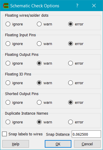
The Check Options dialog sets the Check CellView options. For each option, you can set the check to either ignore the result, issue a warning or issue an error. Floating wires/solder dots checks for any wires or solder dots that are unconnected to device pins or external pins. Floating Input Pins checks for pins with direction Input that are not connected to device pins. Floating Output Pins checks for pins with direction Output that do not connect to device pins. And similarly Floating IO Pins checks for pins with direction Inout that are not connected to device pins. Shorted Output Pins checks for output pins of devices that share a net with other output pins of devices. Duplicate Instance Names checks for instances with the same name.
The Map Devices menu allows mapping a cell in the schematic to a different named cell (usually pcell) in the layout.
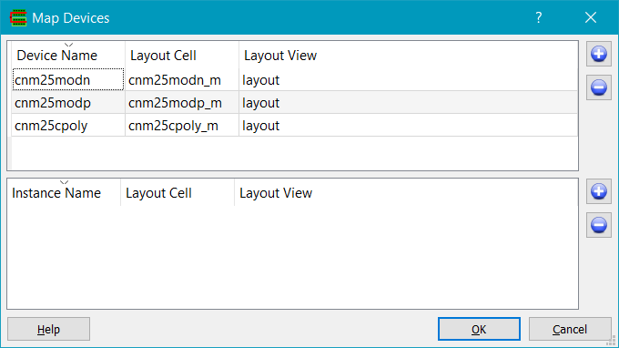
In the above dialog, the entries in the Device Name section of the table map a cell such as cnm25modn in the schematic to a cell called cnm25modn_m in the layout. Entries in the Instance Name section can map specific instances of a cell to a different layout cell.
Device mapping can be set up to pre-seed the dialog using entries in the Glade technology file:
MAP cnm25modn TO cnm25modn_m layout ;
MAP cnm25modp TO cnm25modp_m layout ;
MAP cnm25cpoly TO cnm25cpoly_m layout ;
To create a layout view from a schematic, use the Create Layout command.
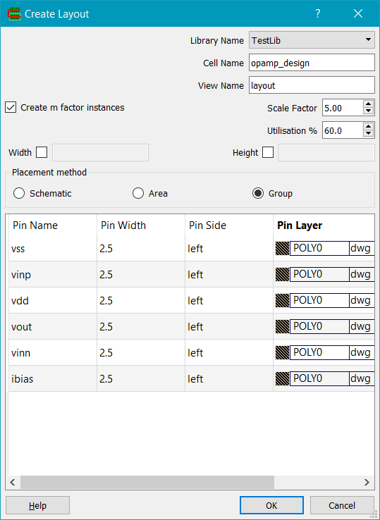
The target cellView is specified using the Library Name / Cell Name / View Name fields. If Create m factor instances is set, then if a schematic instance has an integer property 'm', then multiple instances of the cell will be created in the layout based on the value of the property, and the m property is not passed to the layout pcell. If not checked, the m property is passed to the layout pcell, if the pcell is required to handle this itself.
Scale Factor is used when the placement method is Schematic. It scales the instance origin coordinates by the factor, so the resulting layout mimics the schematic. The actual value required will depend on the target library cells.
Utilisation is used to create the cell boundary layer in the resulting layout view. The area of all the layout instances is summed, and divided by 100/utilisation%. If Width is specified, the cell boundary will be rectangular with the specified width, and height will be computed from the area/width. If Height is specified, the cell boundary rectangle will have the specified height and the width will be computed from the area/height. If both Width and Height are speciified, then the cell boundary rectangle will use the specified width and height.
Placement method can be one of Schematic, Area or Group. Schematic placement uses the relative coordinates of the schematic instance origins to place the layout cells. Area arranges the layout cells by type (PMOS/NMOS/resistor/capacitor). Group will place cells according to group properties on the schematic.
The pin field allows pin width, side and layer to be specified for each pin. Pins are placed abutting the cell boundary rectangle according to their side.
Create Group takes a selected set of instances and creates a group for group placement in Gen Layout. A property with name "group" and value given by the group name will be created on all the selected instances.
Add to Group will add selected instances to the specified group.
Remove from Group will remove the selected instances from the specified group.
Delete Group will delete the specified group. All instances of that group will have the property named "group" removed.
Layout->Rename Group
Rename Group will take an existing group and rename it.
Edit Group allows setting the pattern for the layout of the group's instances.
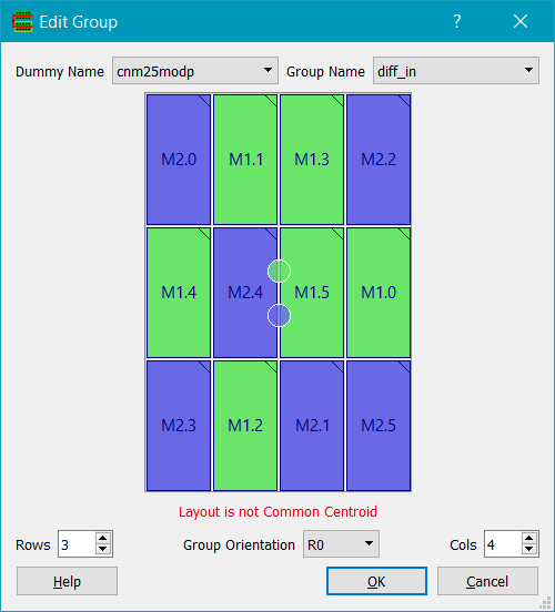
The instances of the group specified by Group Name are displayed as a grid, with different instance basenames in different colours (an instance basename is the name as seen on the schematic e.g. M6; the full name e.g. M6.0 consists of the basename and optionally the individual instances expanded by m-factor as <basename>.0, <basename>.1 etc). The Rows and Cols spinboxes can be used to change the generated array of devices; the size of the array is always greater than the number of actual instances. Dummy Name is the name of the cellView to use for adding dummy cells. Group Name sets the current group to edit. To change positions of instances, left click and drag an instance to a new position; the source and destination instances are swapped.
For groups with more than one instance basename, the centre of gravity of the instances are shown by a circle,
coloured with the instance colour. If all instances centres of gravity coincide, then the layout pattern is
shown as being common centroid with the label in green. If not, the label indicator is red.
Right clicking on an instance displays a context menu with options to mirror or rotate the device and to add
dummies before or after the current selected instance, and to delete a currently selected dummy. Dummies are
given the prefix IDMY to the instance name, followed by a period and a number which is incremented for each
dummy that is added. Dummy cells are generated as instances of cells with the cell master specified by Dummy
Name. Dummies are not (yet) backannotated to the schematic and are not assigned connectivity. Instance
orientations are shown by the tab triangle which is in the top right for orientation R0, top left for MY
etc. Rows and Cols set the size of the group; as one is altered the other is also so that
the overall cell count is approximately maintained. Group Orientation is a global orientation of
the group and takes effect as a transformation of all instances after any instance-specific mirroring.
The group patterns are saved to the schematic cellView as a property with name equal to the group name. The
value of this property is a string of the form "I0.0_0_0_0,I0.1_0_1_6" etc. where each field
delimited by a comma represents the instance name, the row number and the column number, finally the
orientation as a digit, delimited by an underscore.
Link to Layout sets the mapping from schematic to layout. If you have two windows open in MDI mode, one for the schematic and one for the layout, this allows cross probing between layout instances and schematic instances. The corresponding instances are selected in the linked cellview, and are highlighted. Note that layout linking is automatically carried out when Gen Layout is run.
Clears highlighted instances.
Copyright © Peardrop Design 2026.